Core Competency
Photolithography Process
Photolithography Process Introduction
With the widespread use of various high-speed streaming data signals, higher frequency clock signal sources are required; however, the traditional mechanical method can no longer meet the higher frequency requirements. Thus, the photolithography process was applied to the quartz wafer industry, enabling high frequency, miniaturization, and high-precision products to be realized. Process introduction as below
01
Adopting photo-etching method, it's easy to process tens of thousands of blanks in a batch to achieved target frequency on wafer level.

02
Same as above, on wafer level, we can processing tens of thousands blanks in a batch and complete outer frame, and the photo-etching method is used to easily miniaturize the product, with higher dimensional consistency and higher precision.

03
Same as above, on wafer level, we use the same method to process circuit.

Why Photolithography?
Miniaturization
(current min 0806)
Adopting semiconductor process to meet customer demand for miniaturized products
High Frequency
(max500MHz)
3D structure design strengthen the rigidity of blank to meet high frequency demand of customers
High Precision
(Accuracy 2um)
Production by batch, precise size and shape control to meet uniformity for electrical and quality stability
Photolithography Process Overcomes Technical Barriers of High Frequency Blank

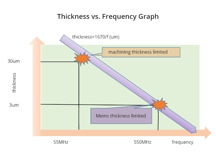
Since the maximum thickness of quartz blank by mechanical process is about 30um (55MHz), higher frequency blanks (generally 55MHz above) need to use photo-etching process to overcome technical obstacles.
*
The thinner the thickness of the quartz blank, the higher the frequency of the crystal unit. Traditional blank uses mechanical process (machining), and it's thickness
limitation is about 30um (55MHz)
*
Using photolithography process enable us to do 3D structure design, ladder structure and groove structure, which strengthen blank rigidity, increase design flexibility in thickness and make it easier to miniaturize products and achieve higher frequency with better performance.

Because the thickness of high frequency blank is too thin, the rigidity of blank is not enough. Using photolithography process, the blank structure can be designed in 3D ladder structure, the thickness of oscillation area will be not limited. This method can achieve 3~30um in general as shown in following figures:
Traditional Blank & Photolithography Blank Comparison
Quality Comparison
The stability and precision of photolithography process are better than those of traditional process, and the quality consistency is much higher.
Photolithography Advantage :
1. Batch production, high stability
2. Photo-etching process, easy to meet miniaturization, thinning, high precision requirement.

Traditional Process :
1. First, cutting quartz column by 2 times to become quartz blank
2. Then polishing the blank, beveling the blank, and electrode forming
3. Difficulty in thinning and miniaturization.


Electrical Performance Comparison
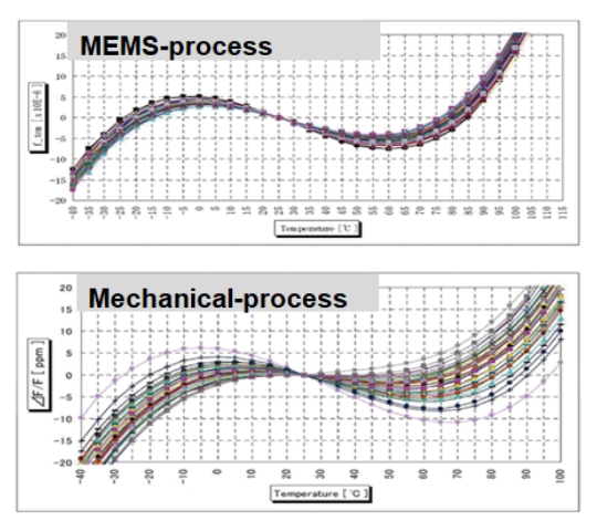
The electrical performance of photolithography process is better than traditional process due to following characteristics. The structure of AT blank made by photolithography, its feature as following :
1. Precise size control
2. 3D structure design
The characteristics of each AT blank by photolithography can reach a stable consistency. Therefore, its frequency curve perform better than traditional process shown as figures.
Production Comparison
-
Size Precision1~3μm30~50μm
-
Thickness Limitation3um30um
-
Structure3D2D
-
High FrequencyEasy (achieve max.500MHz)Difficult (frequency limited 60MHz)
-
MiniaturizationEasy (achieve min.0806)Difficult
-
StabilityBetterWorse
