
产品
希华提供各种不同石英晶体元件,具有各种尺寸、广泛的频率范围且高精度的频率振荡和低 ESR。产品包含非主动式元件的 Crystal (晶体)、Thermistor (内置热敏型晶体)、32.768 kHz Tuning Fork (音叉型晶体),及主动元件的振荡器,包含 XO (石英晶体振荡器)、Differential XO (差分石英晶体振荡器)、VCXO (电压控制石英晶体振荡器)、TCXO/VCTCXO (温度补偿/电压控制温度补偿石英晶体振荡器)。产品主要应用于高阶通信、消费性电子、物联网、汽车、工业产业。
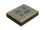
Crystal
晶体谐振器是利用石英晶片镀上膜层之后产生压电效应的一种被动元器件。再将石英晶体加上电压的话,石英水晶会发生形变 (压电效应),从而振动产生接近其固有振动数的稳定且高精度的频率。
Crystal Units (MHz) 32.768 kHz Tuning Fork Crystal Units Crystal Units with Built-in Temperature Sensor (MHz)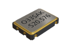
Oscillator
XO (石英晶体振荡器) 是将晶体谐振器与发振电路集成化,产品无温度补偿功能、也无温度控制的最简单的晶体振荡器。其中产品系列别更是有XO、TCXO (温度补偿石英晶体振荡器)、VCXO (电压控制石英晶体振荡器),依据客户使用的模组与系统而有不同的产品可以选用,目前运用于5G网域基础架设、︀资料中心、︀伺服器、︀车用、︀航太卫星。
CMOS Output Oscillator Differential Output Oscillator High-precision Oscillator Low Jitter Oscillator Low Phase Noise Oscillator 32.768 kHz Oscillator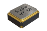
TCXO
TCXO是一种通过内置具有与晶体谐振器温度特性正相反的特性电路 (即温度补偿电路),包含VCTCXO (电压控制温度补偿石英晶体振荡器) ,来获得可覆盖宽温温度范围的温度特性的高精度晶体振荡器。目前运用于GNSS/GPS、︀5G基站、︀航太、︀ADAS。
CMOS Output TCXO Clipped-sine Output TCXO Low Phase Noise TCXO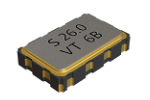
VCTCXO
TCXO是一种通过内置具有与晶体谐振器温度特性正相反的特性电路 (即温度补偿电路),包含VCTCXO (电压控制温度补偿石英晶体振荡器) ,来获得可覆盖宽温温度范围的温度特性的高精度晶体振荡器。目前运用于GNSS/GPS、︀5G基站、︀航太、︀ADAS。
Clipped-sine Output VCTCXO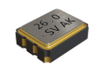
VCXO
VCXO (压控晶体振荡器) 是一种晶体振荡器,其频率由晶体决定,但可以借助施加到输入端的外部控制电压进行调节或调谐。产品用途于 5G 网域基础架设, 基地台。
CMOS Output VCXO
RF Bonded Wafer
Siward engineered Piezoelectric multi layered wafer for RF filter components in requirements demanded by mobile, and other high speed communication. Each substrate of multi-layered wafer, is designed with a view to enable the filter design with high frequency, wide BW, low insertion loss, High Q factor, and TCF (Temperature Coefficient of Frequency) especially for 5G (NR band) performance to mitigate the load of filter design.
RF Bonded Wafer